2025
|
Elahi, Ehsan; Ahsan, Umer; Khan, Muhammad Farooq; Aziz, Jamal; Chauhan, Payal; Michalowski, Pawel Piotr; Chen, Yuan; Eda, Goki; Loula, Martin; Sarkar, Kalyan Jyoti; Sofer, Zdenek Electrical Transport of Nb-Doped MoS2 Homojunction P-N Diode: Investigating NDR and Avalanche Effect Journal Article SMALL, 2025, ISSN: 1613-6810. Abstract | Links | BibTeX @article{ISI:001645762300001,
title = {Electrical Transport of Nb-Doped MoS2 Homojunction P-N Diode: Investigating NDR and Avalanche Effect},
author = {Ehsan Elahi and Umer Ahsan and Muhammad Farooq Khan and Jamal Aziz and Payal Chauhan and Pawel Piotr Michalowski and Yuan Chen and Goki Eda and Martin Loula and Kalyan Jyoti Sarkar and Zdenek Sofer},
doi = {10.1002/smll.202509043},
times_cited = {0},
issn = {1613-6810},
year = {2025},
date = {2025-12-24},
journal = {SMALL},
publisher = {WILEY-V C H VERLAG GMBH},
address = {POSTFACH 101161, 69451 WEINHEIM, GERMANY},
abstract = {2D transition metal dichalcogenides (TMDCs) are promising candidates for next-generation nanoelectronics and optoelectronics. Yet, controlling layer number, stacking angle, and interfacial quality in van der Waals (vdW) heterostructures remains challenging, often limiting device performance and reproducibility. Homojunctions formed within a single 2D material can circumvent these issues, but their reliable fabrication and systematic exploration of exotic quantum phenomena remain elusive. Here, we report the fabrication and characterization of a thickness-modulated lateral p-n homojunction from a single flake of Nb-doped MoS2. This configuration suppresses interface traps without external interface engineering, enabling excellent and highly stable device performance. The diodes exhibit strong rectifying behavior with a rectification ratio of approximate to 10(4) and a remarkably low ideality factor (eta = 1.23). Notably, we observe field-dependent negative differential resistance (NDR) at low temperatures, offering unique prospects for unconventional electronic applications. The devices also achieve high photoresponsivity (1.09 x 10³ A W-1), external quantum efficiency (2.16 x 10(5)%), and detectivity (7.5 x 10¹⁰ Jones). Furthermore, electrical breakdown studies reveal avalanche multiplication at relatively low voltages, enabling high-performance avalanche photodetectors. Overall, our results demonstrate a simple yet robust approach for probing carrier multiplication in 2D homojunction p-n diodes, underlining the broad potential of TMDCs in advanced optoelectronic and quantum device applications.},
keywords = {},
pubstate = {published},
tppubtype = {article}
}
2D transition metal dichalcogenides (TMDCs) are promising candidates for next-generation nanoelectronics and optoelectronics. Yet, controlling layer number, stacking angle, and interfacial quality in van der Waals (vdW) heterostructures remains challenging, often limiting device performance and reproducibility. Homojunctions formed within a single 2D material can circumvent these issues, but their reliable fabrication and systematic exploration of exotic quantum phenomena remain elusive. Here, we report the fabrication and characterization of a thickness-modulated lateral p-n homojunction from a single flake of Nb-doped MoS2. This configuration suppresses interface traps without external interface engineering, enabling excellent and highly stable device performance. The diodes exhibit strong rectifying behavior with a rectification ratio of approximate to 10(4) and a remarkably low ideality factor (eta = 1.23). Notably, we observe field-dependent negative differential resistance (NDR) at low temperatures, offering unique prospects for unconventional electronic applications. The devices also achieve high photoresponsivity (1.09 x 10³ A W-1), external quantum efficiency (2.16 x 10(5)%), and detectivity (7.5 x 10¹⁰ Jones). Furthermore, electrical breakdown studies reveal avalanche multiplication at relatively low voltages, enabling high-performance avalanche photodetectors. Overall, our results demonstrate a simple yet robust approach for probing carrier multiplication in 2D homojunction p-n diodes, underlining the broad potential of TMDCs in advanced optoelectronic and quantum device applications. |
Zhu, Bin; Tang, Jiulin; Cao, Qichao; Zhang, Nan; Yu, Xiaoan; Zhang, Kaisheng; Du, Hui; Li, Zhuo; Peng, Yanhua; Gao, Ruitong; Cai, Haoyuan; Yu, Xue-fang; Cheng, Jianbo; Yang, Xiaolong Photothermal synergistic catalysis on Zr-doped ZnIn2S4 for mild alcoholysis of epoxides: Atomic-level acidity-basicity modulation and carrier dynamics steering Journal Article CHEMICAL ENGINEERING JOURNAL, 525 , 2025, ISSN: 1385-8947. Abstract | Links | BibTeX @article{ISI:001641335200012,
title = {Photothermal synergistic catalysis on Zr-doped ZnIn2S4 for mild alcoholysis of epoxides: Atomic-level acidity-basicity modulation and carrier dynamics steering},
author = {Bin Zhu and Jiulin Tang and Qichao Cao and Nan Zhang and Xiaoan Yu and Kaisheng Zhang and Hui Du and Zhuo Li and Yanhua Peng and Ruitong Gao and Haoyuan Cai and Xue-fang Yu and Jianbo Cheng and Xiaolong Yang},
doi = {10.1016/j.cej.2025.170765},
times_cited = {0},
issn = {1385-8947},
year = {2025},
date = {2025-12-01},
journal = {CHEMICAL ENGINEERING JOURNAL},
volume = {525},
publisher = {ELSEVIER SCIENCE SA},
address = {PO BOX 564, 1001 LAUSANNE, SWITZERLAND},
abstract = {The conventional nucleophilic addition of alcohols to epoxides for producing valuable beta-alkoxy alcohols typically requires strong acids and harsh conditions, hindering green synthesis under mild alternatives. Inspired by recent advances in photo-thermal-synergistic systems for energy and environmental applications, this work synthesized Zr-doped ZnIn2S4 (Zr-ZnIn2S4) nanosheets as a novel photothermal catalyst for the mild alcoholysis of epoxides. Remarkably, the optimal 2 % Zr-ZnIn2S4 catalyst achieved a 98.9 % yield for styrene oxide alcoholysis with isopropanol under blue light illumination at 80 degrees C. Structural characterization revealed that Zr doping modulated the electronic structure of ZnIn2S4, significantly enhancing surface acidity and basicity while simultaneously suppressing photogenerated carrier recombination through shallow-trap defects. The abundant exposed Zn/Zr sites functioned as acidic centers, facilitating the adsorption and polarization of epoxides-identified as the rate-determining step for pristine ZnIn2S4. Ultimately, the efficient separation of photogenerated carriers cooperatively promoted the nucleophilic addition reactions (SN1 and SN2) between the epoxide (styrene oxide or epichlorohydrin) and alcohol. This study provides deep insights into the atomic-level site design of Zr-Zn-In-S photothermal catalysts for achieving photothermal synergistic-driven organic transformations via photo-redox catalysis.},
keywords = {},
pubstate = {published},
tppubtype = {article}
}
The conventional nucleophilic addition of alcohols to epoxides for producing valuable beta-alkoxy alcohols typically requires strong acids and harsh conditions, hindering green synthesis under mild alternatives. Inspired by recent advances in photo-thermal-synergistic systems for energy and environmental applications, this work synthesized Zr-doped ZnIn2S4 (Zr-ZnIn2S4) nanosheets as a novel photothermal catalyst for the mild alcoholysis of epoxides. Remarkably, the optimal 2 % Zr-ZnIn2S4 catalyst achieved a 98.9 % yield for styrene oxide alcoholysis with isopropanol under blue light illumination at 80 degrees C. Structural characterization revealed that Zr doping modulated the electronic structure of ZnIn2S4, significantly enhancing surface acidity and basicity while simultaneously suppressing photogenerated carrier recombination through shallow-trap defects. The abundant exposed Zn/Zr sites functioned as acidic centers, facilitating the adsorption and polarization of epoxides-identified as the rate-determining step for pristine ZnIn2S4. Ultimately, the efficient separation of photogenerated carriers cooperatively promoted the nucleophilic addition reactions (SN1 and SN2) between the epoxide (styrene oxide or epichlorohydrin) and alcohol. This study provides deep insights into the atomic-level site design of Zr-Zn-In-S photothermal catalysts for achieving photothermal synergistic-driven organic transformations via photo-redox catalysis. |
Liu, Matthew W -J; Ulman, Kanchan Ajit; Zheng, Boyang; Jain, Arpit; Heintzelman, Daniel J; Wang, Ke; He, Wen; Dong, Chengye; Lu, Li-Syuan; Crespi, Vincent H; Quek, Su Ying; Robinson, Joshua A; Jr, Kenneth Knappenberger L Structure-Dependent Electronic Relaxation Dynamics of Two-Dimensional Silver Monolayers Journal Article NANO LETTERS, 25 (49), pp. 17145-17151, 2025, ISSN: 1530-6984. Abstract | Links | BibTeX @article{ISI:001629007700001,
title = {Structure-Dependent Electronic Relaxation Dynamics of Two-Dimensional Silver Monolayers},
author = {Matthew W -J Liu and Kanchan Ajit Ulman and Boyang Zheng and Arpit Jain and Daniel J Heintzelman and Ke Wang and Wen He and Chengye Dong and Li-Syuan Lu and Vincent H Crespi and Su Ying Quek and Joshua A Robinson and Kenneth Knappenberger L Jr},
doi = {10.1021/acs.nanolett.5c04723},
times_cited = {0},
issn = {1530-6984},
year = {2025},
date = {2025-12-01},
journal = {NANO LETTERS},
volume = {25},
number = {49},
pages = {17145-17151},
publisher = {AMER CHEMICAL SOC},
address = {1155 16TH ST, NW, WASHINGTON, DC 20036 USA},
abstract = {The electronic relaxation dynamics of two-dimensional silver polar metal heterostructures (2D-PMets), isolated with two different Ag lattice structures, were studied with femtosecond transient absorption (fs-TA) spectroscopy. The two 2D Ag phases, called Ag-(1) and Ag-(2), differ in atomic packing density, which leads to phase-specific ultralow frequency (ULF) phonon modes and visible electronic absorption transitions. Time-resolved kinetic traces for both phases were fit to a biexponential decay function, with the first decay component pertaining to ultrafast electronic relaxation and the second corresponding to carrier-phonon scattering. The first decay time constant tau(1) is <400 fs for both phases. In contrast, carrier-phonon scattering exhibited lattice-specific and excitation wavelength-independent relaxation time constants; tau(2) similar to 2 ps for Ag-(1) and similar to 1 ps for Ag-(2). The shorter tau(2) in Ag-(2) is attributed to increased carrier-phonon scattering probability in more close-packed lateral structures. The results indicate that atomic-level structure controls energy flow in spatially confined 2D materials.},
keywords = {},
pubstate = {published},
tppubtype = {article}
}
The electronic relaxation dynamics of two-dimensional silver polar metal heterostructures (2D-PMets), isolated with two different Ag lattice structures, were studied with femtosecond transient absorption (fs-TA) spectroscopy. The two 2D Ag phases, called Ag-(1) and Ag-(2), differ in atomic packing density, which leads to phase-specific ultralow frequency (ULF) phonon modes and visible electronic absorption transitions. Time-resolved kinetic traces for both phases were fit to a biexponential decay function, with the first decay component pertaining to ultrafast electronic relaxation and the second corresponding to carrier-phonon scattering. The first decay time constant tau(1) is <400 fs for both phases. In contrast, carrier-phonon scattering exhibited lattice-specific and excitation wavelength-independent relaxation time constants; tau(2) similar to 2 ps for Ag-(1) and similar to 1 ps for Ag-(2). The shorter tau(2) in Ag-(2) is attributed to increased carrier-phonon scattering probability in more close-packed lateral structures. The results indicate that atomic-level structure controls energy flow in spatially confined 2D materials. |
Shi, Lu; Zhang, Hanning; Grebenko, Artem K; Yamaletdinov, Ruslan; Rejaul, S K; Shivajirao, Ranjith; Tong, Zheng Jue; Luchkin, Sergey; Zhang, Hongji; Iakoubovskii, Konstantin V; Alekseeva, Alena A; Starkov, Andrei; Orofeo, Carlo M; Lin, Junhao; Suenaga, Kazutomo; Toh, Chee-Tat; Mahfouz, Remi; Tayeb, Talah M; Qari, Nada; Adams, Stefan; Weber, Bent; Yazyev, Oleg V; Ozyilmaz, Barbaros Monolayer Amorphous Carbon: Unlocking Disorder-Induced Lithiophilicity Journal Article ADVANCED SCIENCE, 2025. Abstract | Links | BibTeX @article{ISI:001622287600001,
title = {Monolayer Amorphous Carbon: Unlocking Disorder-Induced Lithiophilicity},
author = {Lu Shi and Hanning Zhang and Artem K Grebenko and Ruslan Yamaletdinov and S K Rejaul and Ranjith Shivajirao and Zheng Jue Tong and Sergey Luchkin and Hongji Zhang and Konstantin V Iakoubovskii and Alena A Alekseeva and Andrei Starkov and Carlo M Orofeo and Junhao Lin and Kazutomo Suenaga and Chee-Tat Toh and Remi Mahfouz and Talah M Tayeb and Nada Qari and Stefan Adams and Bent Weber and Oleg V Yazyev and Barbaros Ozyilmaz},
doi = {10.1002/advs.202516490},
times_cited = {0},
year = {2025},
date = {2025-11-25},
journal = {ADVANCED SCIENCE},
publisher = {WILEY},
address = {111 RIVER ST, HOBOKEN 07030-5774, NJ USA},
abstract = {Dendritic lithium growth on the current collector remains a major obstacle to developing anode-less batteries, arising from inhomogeneous lithium nucleation and uneven surface lithiophilicity. Existing approaches, such as metallic or carbonaceous interlayers, often fail to stabilize lithium deposition due to mechanical degradation or spatial variations in lithium affinity. Here, we demonstrate that a monolayer amorphous carbon (MAC) film-a single-atom-thick disordered sp2 network grown directly on copper-can fundamentally alter lithium nucleation behavior. The topological disorder of MAC produces a dense distribution of electron-rich sites that uniformly strengthen lithium binding. As a result, the MAC surface exhibits a lithium contact angle of 31 +/- 5 degrees, four times lower than that of graphene and nearly three times lower than that of bare copper, leading to homogeneous wetting and deposition. Electrochemical tests reveal a reduced nucleation overpotential of 28.9 mV at 0.5 mA cm-2. Density functional theory and scanning tunneling microscopy confirm that disorder-induced localization of states near the Fermi level enhances electronegativity and forms continuous lithium-binding sites. These findings establish intrinsic structural disorder, rather than chemical doping, as an effective route to designing uniformly lithiophilic current collectors for next-generation anode-less batteries.},
keywords = {},
pubstate = {published},
tppubtype = {article}
}
Dendritic lithium growth on the current collector remains a major obstacle to developing anode-less batteries, arising from inhomogeneous lithium nucleation and uneven surface lithiophilicity. Existing approaches, such as metallic or carbonaceous interlayers, often fail to stabilize lithium deposition due to mechanical degradation or spatial variations in lithium affinity. Here, we demonstrate that a monolayer amorphous carbon (MAC) film-a single-atom-thick disordered sp2 network grown directly on copper-can fundamentally alter lithium nucleation behavior. The topological disorder of MAC produces a dense distribution of electron-rich sites that uniformly strengthen lithium binding. As a result, the MAC surface exhibits a lithium contact angle of 31 +/- 5 degrees, four times lower than that of graphene and nearly three times lower than that of bare copper, leading to homogeneous wetting and deposition. Electrochemical tests reveal a reduced nucleation overpotential of 28.9 mV at 0.5 mA cm-2. Density functional theory and scanning tunneling microscopy confirm that disorder-induced localization of states near the Fermi level enhances electronegativity and forms continuous lithium-binding sites. These findings establish intrinsic structural disorder, rather than chemical doping, as an effective route to designing uniformly lithiophilic current collectors for next-generation anode-less batteries. |
Fu, Deyi; Liu, Jiawei; Hou, Fuchen; Chang, Xiao; Qu, Tingyu; Felisaz, Johan; Krishnaswamy, Gunasheel Kauwtilyaa; Grebenchuk, Sergey; Jie, Yuang; Watanabe, Kenji; Taniguchi, Takashi; Pereira, Vitor M; Novoselov, Kostya S; Koperski, Maciej; Yakovlev, Nikolai L; Soumyanarayanan, Anjan; Avsar, Ahmet; Yazyev, Oleg V; Lin, Junhao; Ozyilmaz, Barbaros Electric field-tunable ferromagnetism in a van der Waals semiconductor up to room temperature Journal Article NATURE COMMUNICATIONS, 16 (1), 2025. Abstract | Links | BibTeX @article{ISI:001620530800035,
title = {Electric field-tunable ferromagnetism in a van der Waals semiconductor up to room temperature},
author = {Deyi Fu and Jiawei Liu and Fuchen Hou and Xiao Chang and Tingyu Qu and Johan Felisaz and Gunasheel Kauwtilyaa Krishnaswamy and Sergey Grebenchuk and Yuang Jie and Kenji Watanabe and Takashi Taniguchi and Vitor M Pereira and Kostya S Novoselov and Maciej Koperski and Nikolai L Yakovlev and Anjan Soumyanarayanan and Ahmet Avsar and Oleg V Yazyev and Junhao Lin and Barbaros Ozyilmaz},
doi = {10.1038/s41467-025-59961-2},
times_cited = {0},
year = {2025},
date = {2025-11-20},
journal = {NATURE COMMUNICATIONS},
volume = {16},
number = {1},
publisher = {NATURE PORTFOLIO},
address = {HEIDELBERGER PLATZ 3, BERLIN, 14197, GERMANY},
abstract = {Ferromagnetic semiconductors, coupling charge transport and magnetism via electrical means, show great promise for spin-based logic devices. Despite decades of efforts to achieve such co-functionality, maintaining ferromagnetic order at room temperature remains elusive. Here, we address this long-standing challenge by implanting dilute Co atoms into few-layer black phosphorus through atomically-thin boron nitride diffusion barrier. Our Co-doped black phosphorus-based devices exhibit ferromagnetism up to room temperature while preserving its high mobility (similar to 1000cm(2)V(-1)s(-1)) and semiconducting characteristics. By incorporating ferromagnetic Co-doped black phosphorus into magnetic tunnel junction devices, we demonstrate a large tunnelling magnetoresistance that extends up to room temperature. This study presents a new approach to engineering ferromagnetic ordering in otherwise nonmagnetic materials, thereby expanding the repertoire and applications of magnetic semiconductors envisioned thus far.},
keywords = {},
pubstate = {published},
tppubtype = {article}
}
Ferromagnetic semiconductors, coupling charge transport and magnetism via electrical means, show great promise for spin-based logic devices. Despite decades of efforts to achieve such co-functionality, maintaining ferromagnetic order at room temperature remains elusive. Here, we address this long-standing challenge by implanting dilute Co atoms into few-layer black phosphorus through atomically-thin boron nitride diffusion barrier. Our Co-doped black phosphorus-based devices exhibit ferromagnetism up to room temperature while preserving its high mobility (similar to 1000cm(2)V(-1)s(-1)) and semiconducting characteristics. By incorporating ferromagnetic Co-doped black phosphorus into magnetic tunnel junction devices, we demonstrate a large tunnelling magnetoresistance that extends up to room temperature. This study presents a new approach to engineering ferromagnetic ordering in otherwise nonmagnetic materials, thereby expanding the repertoire and applications of magnetic semiconductors envisioned thus far. |


 10OctOctober InnovaTalk webinar: “Smart Materials for Energy Harvesting and Storage”Read More
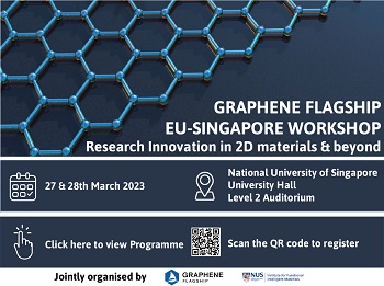 27MarThe 1st Graphene Flagship EU-Singapore Workshop on Graphene and related 2D MaterialsRead More
 22SepTowards three-dimensional atom-by-atom imaging by STEM depth sectioningRyo Ishikawa is a Project Associate Professor at the Institute of Engineering Innovation at the University of Tokyo, Japan. He completed his Ph.D. inRead More
 26JulTurning on the heat with spins and their transport across interfacesHari Srikanth is a Distinguished University Professor at the University of South Florida. He received his Ph.D. in experimental condensed matter physiRead More
 20AprTowards Single Atom Catalysis for Environmental ApplicationJaehong Kim is currently Henry P. Becton Sr. Professor of Engineering and Department Chair of Chemical and Environmental Engineering in School of EngiRead More