
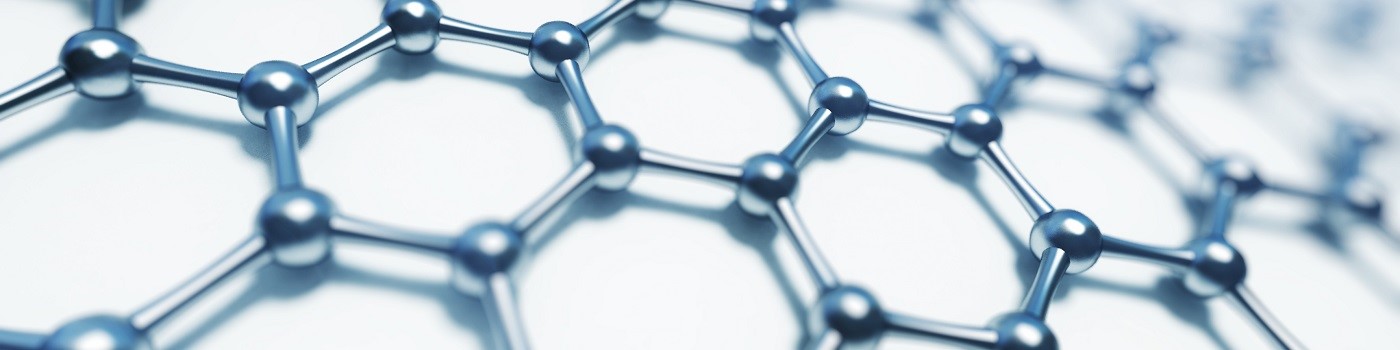
Graphene
Graphene research is a relatively young field, being “founded” in 2004-2005 by a series of papers that involved several groups around the world including the Manchester and Columbia groups. Graphene was quickly recognized as an interesting material because there was an entire community of researchers working on related materials, namely, graphite, fullerenes, and carbon nanotubes. All these materials can be thought as directly related to graphene (graphite = stacked graphene, fullerenes = wrapped graphene, nanotubes = rolled graphene – see Fig.1). It was relatively simple for these researchers to move from an area that was scientifically saturated to a new one with minimal amount of investment in terms of resources and, especially, time.
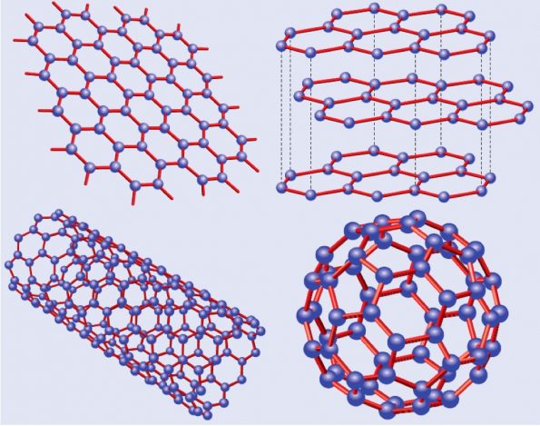
Fig 1. Graphene and its descendants: top right: graphene; top left: graphite = stacked graphene; bottom right: nanotube=rolled graphene; bottom left: fullerene=wrapped graphene (adapted from ref.[1]).2
Ludwig Wittgenstein once commented that “the aspects of things that are most important to us are hidden because of their simplicity and familiarity”. In fact, graphene has been hidden behind the pencil trace since the it was invented in 1656 in England. One can say that this one atom thick material is being produced by human beings since the 17 th century but only recently, after more than 400 years, we were really able study its properties closely. This material always had an economic appeal, in the 17 th century for the the production of pencils, now in the 21st century as the next material of choice for high-end flexible electronics.
With the benefit of hindsight, it is not surprising that this one atom thick material was extracted from graphite with an adhesive tape. However, a large the amount of work had to be done to bring graphene to the high standards of modern nanotechnology. Without clean-room facilities, e-beam lithography, or scanning electron microscopy, the discoveries made in the last 5 years would not be possible. The rapid evolution in nanotechnology in the last decade is what allowed for the experiments that opened the doors for the understanding of the unusual properties of this material (see Fig.2).
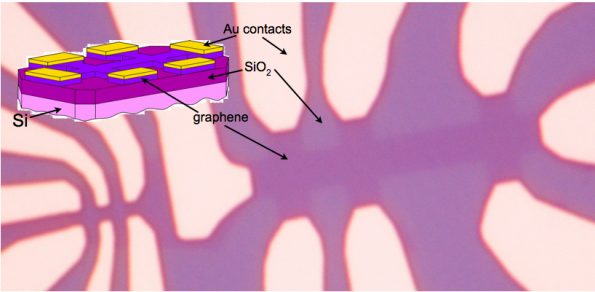
Fig 2: Graphene device: optical picture of a graphene device made out of a lithographically cut graphene sheet on top of SiO2, with gold electrodes and a doped Si back gate.
We note that it was quite obvious from the very beginning that mechanical exfoliation (the so-called “scotch tape” method) is a big limitation for the use of this material in applications, that is, one would have to develop a mass production method. In fact, even before 2004, many researchers worked on the growth of graphene by artificial means. The growth out of SiC, for instance, is considered one of most promising ways to produce large area graphene for electronic applications. More recently, chemical vapor deposition (or CVD), has become extremely popular because of its simplicity and low cost (and possibly its interesting environmental impact: CO2 capture for graphene production). Each method has its pros and cons: strong interaction with the substrate can lead to large charge transfer and difficulties in transferring the material to an appropriate (say, flexible) substrate; mechanical stability during the transfer process to plastic (for flexible electronics) can lead to structural failure; formation of extended defects due to heterogeneous growth can reduce the electronic mobility. Only time and investment can tell which of these methods will be the dominant one in the industrial use of graphene. The fact of the mater is that today it is possible to produce large area graphene (even square meters) using CVD with reasonable electronic mobilities (> 5,000 cm2/Vs). Hence, it is clear that the barrier for large area production has been broken. This is not to say that much development is still needed to make the material of the highest quality (single crystal) given that the CVD growth is heterogenous and produces polycrystalline samples.
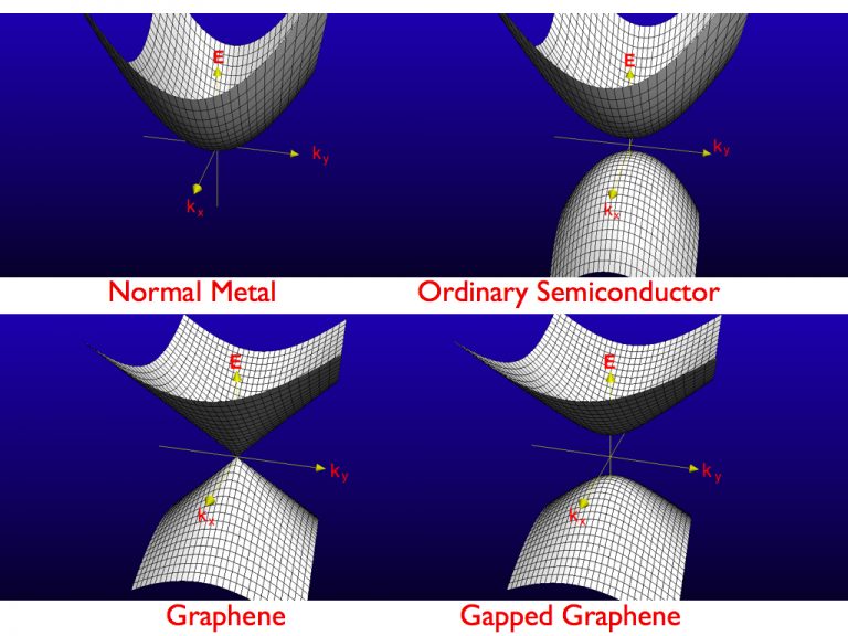
One of the most important properties of graphene comes from its unusual electronic excitations that can be described in terms of massless two-dimensional Dirac particles (see Ref.[2] for more details). The interference between electronic waves, as they propagate through the graphene crystal, that allows for this unusual electronic behavior. Hence, the “diracness” of the electrons in graphene is “protected” by crystal symmetry. At low energies and long wavelengths, the electrons in graphene are not characterized by their mass but by their speed of propagation, the so-called Fermi-Dirac velocity, which is of the order of 106 m/s (that is, approximately 300 times smaller than the speed of light). At low energies, the electrons in graphene obey a relativistic wave equation in two dimensions. This property created a heated interest in the theoretical community. From the point of view of solid state physics, however, graphene is also interesting because its electronic density of states vanishes linearly with energy at the Dirac point. Thus, neutral graphene is a strange material, a mix between a metal and an insulator. Graphene is not a metal because it has a vanishing density of states. Graphene is not also a semiconductor (or insulator) because it does not have a gap in the spectrum. Thus, unlike a semiconductor, it does not have a threshold for electronic excitations.
Also from the structural point of view, graphene is not an ordinary material. The interaction between carbon atoms is made through strong sigma bonds (similar to the ones in diamond) through the overlap of the in-plane sp2 orbitals. Because of that, graphene has a very high spring constant, K (~ 50 eV/Å2), and its Young modulus, Y (~ 1 TPa), is one of the largest in nature. As a result, its optical phonon frequencies, ω0 (~ 0.2 eV ~ 1,600 cm-1), are one of the highest among all materials.
Another fascinating property of graphene is related with its softness. Because the material is only one atom thick, it can be easily deformed in the direction normal to its surface. In the absence of any external constraints (such as substrates, scaffolds, impurities, etc), graphene can sustain “flexural phonon” modes whose frequency, ωF, is a quadratic function of the wavevector, q (ωF(q) = (κ/σ)1/2 q2, where κ ~ 1 eV is the so-called bending rigidity and σ is the surface mass density of graphene). Notice that unlike acoustical phonon modes (that is, sound waves), these modes do not propagate since they have a vanishing group velocity at long wavelengths. These modes represent the displacement of the center of mass of the whole graphene sheet in the direction normal to its surface. The presence of flexural modes is guaranteed by symmetry in all 2D crystals. Hence, 2D crystals are all membranes (albeit with different stiffnesses). In the absence of external effects that break the translation symmetry in the perpendicular direction, it costs zero energy to translate the whole graphene crystal. However, in the presence of terms that break this symmetry, the frequency of the flexural modes is affected. An applied tension, that breaks rotational symmetry, changes the dispersion from parabolic to linear (that is, sound waves appear), and the presence of a scaffold or substrate, that break explicitly translational symmetry, makes these modes dispersionless, that is, it requires energy to move graphene out of its flat configuration.
The extreme membrane-like nature of graphene, together with the tough in-plane sigma bonds, leads to graphene’s negative thermal expansion coefficient (that is, graphene shrinks when it is warmed and it expands when it is cooled). This happens because most of the horizontal displacement of the graphene sheet comes from the flexural modes, with very little contribution from the in-plane phonons. When graphene is cooled, the number of flexural modes is greatly reduced and the horizontal length of the graphene sheet is increased. When graphene is in contact with materials with positive thermal expansion coefficient (which is the case of most 3D solids) many interesting structural effects happen when the temperature is varied. In fact, we can say that graphene is the only example of an electrically conductive membrane and, thus, it unifies topics in hard and soft condensed matter. From this perspective, graphene is writing a new chapter in the solid state textbooks.
These amusing properties have a huge impact in the experimental properties of graphene. The sigma bonds are extremely exclusive and directional and hence do not easily accept foreign atoms. Hence, natural graphene (that is, graphene in the form of graphite) is a very pure material with no extrinsic disorder. Most of disorder found in graphene samples obtained by mechanical exfoliation comes from either molecules or atoms adsorbed in its two surfaces, or by structural deformations (wrinkles, ripples, folds, blisters, etc). Thus, natural graphene has the highest electronic mobility of all electronic materials (>100,000 cm2/Vs at 300 K), much larger than Si (~1,500 cm2/Vs) or “cleaner” semiconductors such as AlGaAs/InGaAs (~8,500 cm2/Vs).
Furthermore, because the optical phonon frequencies are so high, the thermal conductivity of graphene is comparable to that in diamond (~ 50 W/cm.K), one order of magnitude larger than ordinary semiconductors (in Si, for instance, the thermal conductivity is of order 1 cm2/Vs). These unprecedented properties make of graphene a unique material with characteristics that can lead to an enormous number of applications in a large number of different areas, from high end electronics and biosensors to metallic paints and surface impermeabilization.
References
[1] A. H. Castro Neto, F. Guinea, and N. M. R. Peres, ”Drawing conclusions from graphene”, Physics World 19, 33 (2006).
[2] A. H. Castro Neto, F. Guinea, N. M. R. Peres, K. S. Novoselov, and A. K. Geim, “The electronic properties of graphene”, Reviews of Modern Physics 81, 109 (2009).