
Research Areas
The target areas of intervention of the NUS Centre for Advanced 2D Materials are:
- Atomically thin, wafer size, crystal growth, and characterization: Raman, AFM, TEM, STM, magneto transport, angle resolved photoemission (ARPES), optics.
- Flexible electronics and strain engineering of atomically thin materials.
- Mechanics of atomically thin film transfer.
- Nano-scale patterning and new device development.
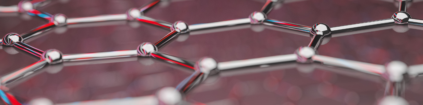
- Three-dimensional architectures based on atomically thin films (atomic multi-layers, see figure).
- Composite materials where accumulated stress could be monitored by contactless, non-invasive, optical methods.
- Spintronics and valleytronics in two-dimensional materials.
- Atomically thin electrodes for photovoltaic or OLED applications.
- Atomically thin gas barriers and electrodes for energy/charge transfer and storage (water splitting, fuel cells, etc).
- Solution-processed atomically thin substrates for bio applications and catalysis.
- Atomically thin films as optical components in fiber lasers (mode locking, polarizers etc).
- Atomically thin film platforms for bio-sensing and stem cell growth.
- Atomically thin film platforms for sol-gel, organic, and electro-chemistry.
- Graphene-ferroelectric memories (G-FeRAM), graphene spin torque transistors (G-STT).
- Computational modeling of new atomically thin materials and complex architectures.