Our Solutions
The Centre for Advanced 2D Materials has built a state-of-the-art clean room facility with 800 m2 of Class 1000 and 100 landscapes.
It provides sophisticated micro- and nanofabrication facilities for graphene and other research material.
X-ray Photoelectron Spectroscopy (XPS)
X-ray Photoelectron Spectroscopy (XPS)
A powerful method for investigating surface composition and electronic structure

XPS Analysis – X-ray photoelectron Spectroscopy (XPS), also known as Electron Spectroscopy for Chemical Analysis (ESCA), is a powerful analytical technique that provides valuable insights into the elemental and chemical composition of surfaces. Typically using monochromated Al K-alpha excitation, XPS provides quantitative chemical information from the upper most 10 nm of a material. The technique is used in both industrial and academic research, including electronics, semiconductor physics, novel materials and biomaterials, sensor surfaces, surface chemistry and functionalization.
Our Techniques –
- Survey Scan and narrow scan
- Our AXIS SUPRA+ is optimized for chemical state x-ray photoelectron spectroscopy. Efficient collection of photoelectrons combined with high transmission electron optics ensures unrivalled sensitivity and resolution at large analysis areas.
- The survey scan, which identifies the elemental composition of the sample surface.
- Narrow scan, which measures the concentrations of the elements identified in the survey scan. Our AXIS Supra+ is able to scan with high energy resolution, it is critical for the accurate measurement of small chemical shifts.
- Key attributed include:
- Easy detection of light elements
- Excellent signal-to-noise ratio, even at low concentrations
- Fast data acquisition
- Scanned or snap-shot spectral acquisition modes.
- Small Spot Spectroscopy
- Our AXIS Supra+ small spot performance guarantees high sensitivity in small spot mode by optimizing X-ray illumination of the sample within the analysis area selected.
- Key selected area spectroscopy attribute include:
- Pre-defined small spot analysis areas
- Optimised X-ray illumination for improved selected area performance
- Automated aperture and iris in the electrostatic lens column to form a virtual probe at the sample surface
- XPS Imaging
- The lateral distribution of elements or chemistry at the surface is measured by XPS imaging. Our AXIS Supra+ acquires fast, high spatial resolution parallel images. Parallel image acquisition has the advantage that it is significantly faster and achieves higher spatial resolution than the more conventional rastered beam approach.
- Parallel imaging may also be combined with stage movements to acquire a “stitched” image, capable of generating images over several millimeters with spatial resolution of several microns.
- Capabilities provided by parrel imaging include:
- Ultimate spatial resolution of 1 um at the highest magnification.
- High energy resolution, chemical state imaging
- Quantitative imaging – the unique spherical mirror analyser and delay-line detector can provide quantitative chemical state images.
- Spectromicroscopy – easy acquisition of spectra from image dataset providing a spectrum at each pixel.
- Monatomic and Gas Cluster Ion Source
- Our AXIS Supra+ is configured with the Minibeam 6 Gas Cluster Ion Source (GCIS), which is a multi-mode ion source that can operate in Arn+ cluster mode and Ar+/He+ monatomic ion mode as required. It enables depth profiling analysis and surface cleaning of both soft and hard materials on the same XPS instrument.
- With Arn+ cluster ions, it is now possible to perform depth profiles through complex multi-layer materials such as organic LEDs and flexible electronic devices. A unique capability of our Minibeam 6 to generate 20 keV Arn+ cluster ions has allowed the successful etching of inorganic materials such as titanium dioxide with significantly less ion-induced chemical damage.
- Angles-resolved XPS
- Angle-resolved XPS (ARXPS) is an advanced technique that takes XPS analysis to a new level of precision. Typically, the information depth for XPS is a few nanometers, ARXPS, however, is a technique that varies the emission angle at which the electrons are collected, thereby enabling electron detection from different depths. ARXPS provides information about the thickness and composition of thin films, and such measurements are non-destructive, unlike sputter profiling.
- Key attributes with ARXPS:
- A depth profiling of chemical species without destroying the sample
- Can be applied to films that are too thin to be analyzed by conventional depth profiling techniques.
- Ultraviolet Photoelectron Spectroscopy
- Survey Scan and narrow scan
Atomic Force Microscopy (AFM)
Atomic Force Microscopy (AFM)
A powerful measurement tool for surface analysis of materials and active nanoscale systems in air, fluid, electrical or chemically reactive environments.

Atomic Force Microscopy (AFM) is a powerful measurement tool for surface analysis. AFM allows accurate and non-destructive measurements of the topographical, electrical, magnetic, chemical, optical, mechanical, etc. properties of a sample surface with very high resolution in air, liquids or ultrahigh vacuum. This unique combination of capabilities makes AFM indispensable in most advanced science and technology labs around the world.
Measurement Techniques –
- Revolutionary AFM-nDMA
For the first time an AFM can provide complete and quantitative viscoelastic analysis of polymers at the nanoscale, probing materials at rheologically relevant frequencies, in the linear regime. Proprietary dual-channel detection, phase-drift correction, and reference frequency tracking enable a small strain measurement in the rheologically relevant 0.1 Hz to 20 kHz range for nanoscale measurements of storage modulus, loss modulus, and loss tangent that tie directly to bulk DMA.
- Exclusive PeakForce QNM
Quantitative characterization of nanomechanical properties—including modulus, adhesion, dissipation, and deformation — while simultaneously imaging sample topography at atomic-scale resolution has become a routine endeavor with this mode. Now Bruker’s frequency-calibrated probes enable defined geometry and adhesion to track probe-sample contact with the lowest uncertainty in measurements of sticky-soft materials in the <1kPa to 100 GPa range, while rendering results with high-resolution nanoscale mapping. - FASTForce Volume
This mode extends the operating frequency of linear ramps by >400 Hz, closing the frequency gap between
PeakForce QNM and standard Force Volume mapping. The overlap of operating frequencies facilitates nanomechanical correlative studies between modes, rendering greater measurement confidence while allowing investigation of property material frequency dependency. - Innovative FASTForce Volume CR
Due to its ability to measure a wide range of moduli, contact resonance is a powerful tool for nanomechanical measurements. However, until now, its implementation has been hampered by contact mode’s limitations, including slow imaging speed, complex analysis, and the requirement of specialized hardware for full spectrum acquisition. XR Nanomechanics resolves these issues, providing consistent data of both elastic and viscoelastic properties.
Raman Spectroscopy
Raman Spectroscopy
An analytical technique where scattered light is used to measure the vibrational energy modes of a sample, thereby providing a structural fingerprint by which molecules can be identified.
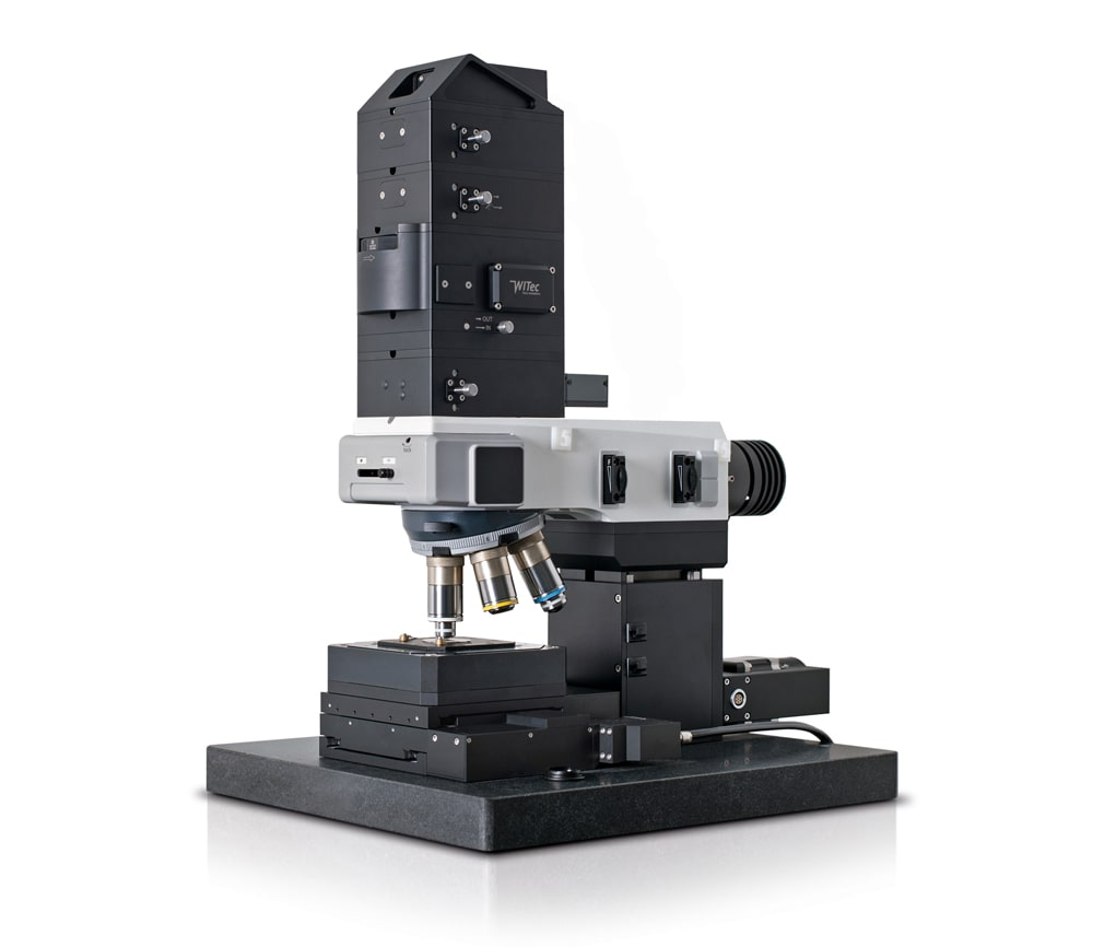
Raman Operation Modes
- Raman spectral imaging: acquisition of a complete Raman spectra at every image pixel
- Planar (x-y-direction) and depth scans (z-direction) with manual sample positioning
- Image stacks: 3D confocal Raman imaging
- Time series
- Single point Raman spectrum acquisition
- Single-point depth profiling
- Fibre-coupled UHTS spectrometer specifically designed for Raman microsopy and applications with low light intensities
- Confocal Fluorescence Microscopy
- Bright Field Microscopy
Scanning Electron Microscopy (SEM) With Energy Dispersive Spectroscopy (EDS)
Scanning Electron Microscopy (SEM) With Energy Dispersive Spectroscopy (EDS)
SEM is a widely used method for imaging microstructure and morphology of materials. Combined with EDS, researchers have a powerful imaging tool that also provides spatially resolved elemental information.

Class-Leading Usability
SmartSEM Touch puts interactive workflow control directly at your fingertips. It is quick and easy to learn, dramatically reducing training effort and costs. Within minutes,
even new users will begin capturing stunning images. This user interface also supports industrial operators who require automated workflows for repeatable inspection tasksExcellent Image Quality
EVO excels at extracting the maximum data quality from uncoated and unaltered samples. EVO also safeguards data quality on hydrated and heavily contaminated samples, by allowing these samples to remain in their native state. Additionally, the LaB6 emitter will give that extra bit of resolution, contrast and signal-to-noise
that is important when imaging and microanalysis get challenging.Automated Intelligent Imaging
EVO enables automated, unattended acquisition of images across sample batches. ZEISS Automated Intelligent Imaging is perfectly suited to routine inspection. It
enables the user to define a boundary region, automatically generate regions of interest determined by the required field of view or magnification, and begin
automated acquisition. Automated Intelligent Imaging will improve your sample throughput, boosting productivity and performance.- Better Data with a Lanthanum Hexaboride (LaB6) Electron Emitter
Electron emission from a lanthanum hexaboride cathode, rather than a traditional tungsten hairpin filament, provides the reassurance that every extra bit of image quality is
there when you need it. And that is a benefit you can put into action in two ways:1. At equivalent electron probe sizes (i.e. resolution), there is more probe current to work with, which makes image navigation and optimization much easier.
2. At equivalent probe currents (signal-to-noise), the beam diameter is much smaller, resulting in enhanced image resolution.
ZEISS SmartEDX is the dedicated microanalysis solution designed specifically for analytical routine applications performed on the ZEISS EVO Family
SmartEDX provides highest (output count rate) throughput at 129 eV energy resolution and 1-5 nA probe current, which is the typical analytical operating condition for the ZEISS EVO Scanning Electron Microscopes.
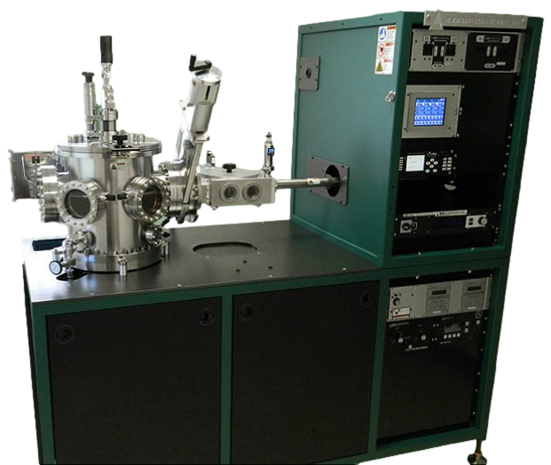
AJA ATC Orion Ultra High Vacuum Electron Beam Evaporator
Compact physical vapor deposition tools for maximum performance.
-
-
-
-
Uniform Deposition Specifically angled con-focal sputter source flange designed based on years of experience, allowing high degree of uniformity over substrates more than twice the target diameter.
-
Magnetron Sputtering Source Cluster Flanges ATC Orion features tuneable isolation chimneys with gas injection and flip-top shutters to accommodate compact spaces and custom chimney designs
-
Substrate holders and heaters Motorised, rotating substrate holders to achieve excellent uniformity. Substrate heaters are able to reach up to 1000°C and features reactive gas injection rings and RF/DC bias capability.
-
-
-
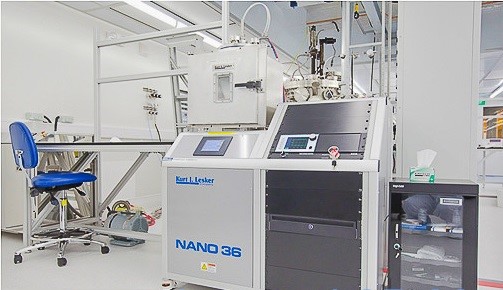
Kurt J Lesker Nano36tm Thermal Evaporator
Reliable, easy to use, compact thin film deposition system
-
-
-
-
Isolated thermal evaporation sources
3 isolated evaporator sources to prevent cross contamination.
-
Wide range of thermal sources
Thermal sources accepted ranges from filaments, basket heaters, box heaters, coated boats, uncoated boats, rods to screens.
-
Ease of use
User friendly graphical user interfaces (GUIs) aids in sample mounting, chamber pressure control and deposition processing.
-
Reliable deposition A quartz crystal sensor is used in conjunction with a thin film controller to ensure reliable deposition at any time.
-
-
-
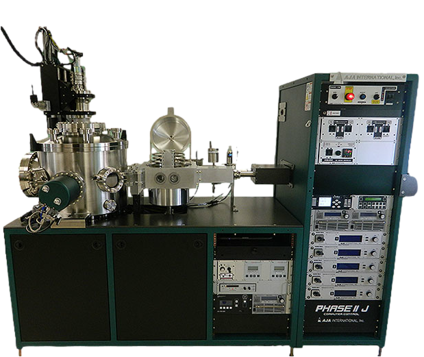
AJA ATC 2200 Ultra High Vacuum Sputtering System
Versatile physical vapor deposition system for precise, repeatable deposition
-
-
-
-
6 magnetron sputtering sources
3 Direct Current (DC) and 3 Alternating Current (AC) sources for deposition of metals and dielectrics.
-
Auto matching Direct Current (DC) and Radio Frequency (RF) generators
DC generator supports up to 750W and RF generator supports up to 300W.
-
8 inch wafer sample holder
Sample holder holds up to a full 8 inch diameter wafer with rotation and DC/RF biasing capabilities.
-
Heater jacket Heater jacket is available for chamber bake-out to obtain Ultra High Vacuum pressure.
-
-
-
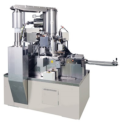
JEOL JBX-6300FS Electron Beam Lithography System
JEOL JBX-6300FS Electron Beam Lithography System
High field stitching and overlay accuracy. High precision pattern writer for R&D of cutting-edge devices and nanotechnology.
-
-
-
-
Highly precise
JBX-6300FS can write highly precise patterns even at field corners and boundaries by the use of its powerful electron optical system that automatically corrects distortions generated by beam deflection.
-
Automatic beam adjustment
JBX-6300FS has an automatic beam adjustment function, enabling beam-dose correction and beam-position correction during pattern writing.
-
High throughput
JEOL JBX-6300FS is a high throughput system running at 25keV, 50keV and 100keV acceleration voltages. -
Multi cassette loader
Able to process piece part samples and 4 inch diameter substrates.
-
Minimum linewidth of 10nm
Minimum linewidth achievable in cleanroom is 10nm with stitching accuracy of less that 20nm at 100keV. JBX-6300FS also comes with Genisys-Beamer software to assist in high resolutions patterning by considering proximity effect.
-
-
-
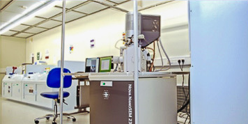
NOVA NanoSEM 230 Ultra-High Resolution SEM (FEI EBL)
NOVA NanoSEM 230 Ultra-High Resolution SEM (FEI EBL)
Ultra-high resolution field emission scanning electron microscope with direct electron beam for nanoprototyping
-
-
-
-
Ultra-high resolution characterisation
NanoSEM 230 is specifically configure to get the most information out of the largest selection of samples, down to nanometer level in high vacuum: 1.6nm @ 1kV. True high resolution low vaccum field emission scanning electron microscope with a resolution of 1.8nm @ 3kV
-
Expanded analysis capabilities
Beam deceleration mode with sub-100V and high surface sensitivity imaging. Superb low and very low kV backscattered electron imaging in high and low vacuum.
-
Full prototyping solution
On board 4k x 4k digital pattern generator, Nabity-NPGS & DesignCAD patterning software, high speed electrostatic beam blanker and gas injection system.
-
-
-
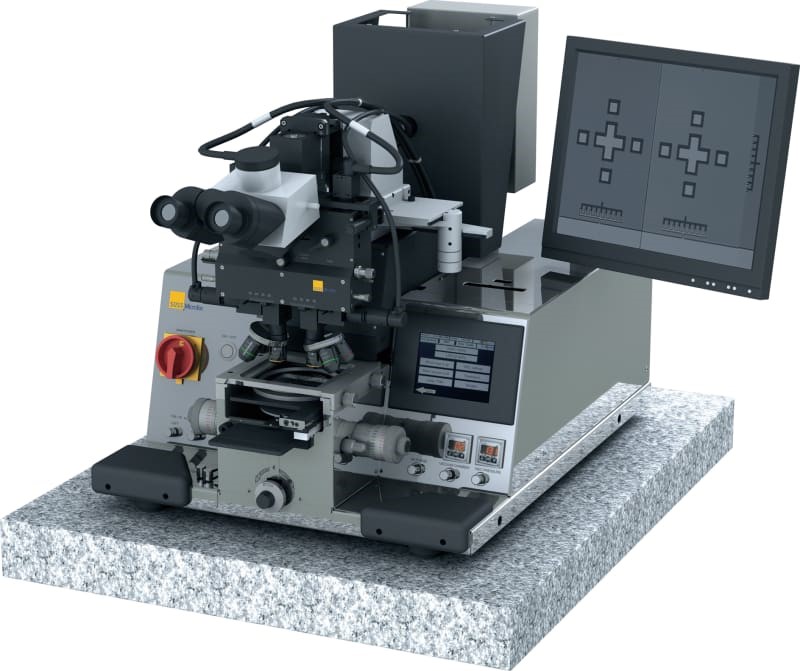
SUSS MicroTec MJB4 Mask Aligner
SUSS MicroTec MJB4 Mask Aligner
Easy to use, compact system for R&D labs and small volume production
-
-
-
-
High resolution printing down to 0.5µm
High resolution optics combined with broadband optics (UV250/300/400) allows for fast switching between wavelengths and high resolution prints
-
Fast and accurate alignment
Fast and highly accurate alignment is achieved with SUSS singlefield or splitfield microscopes
-
Handles small substrates and pieces up to 100mm.
-
-
-
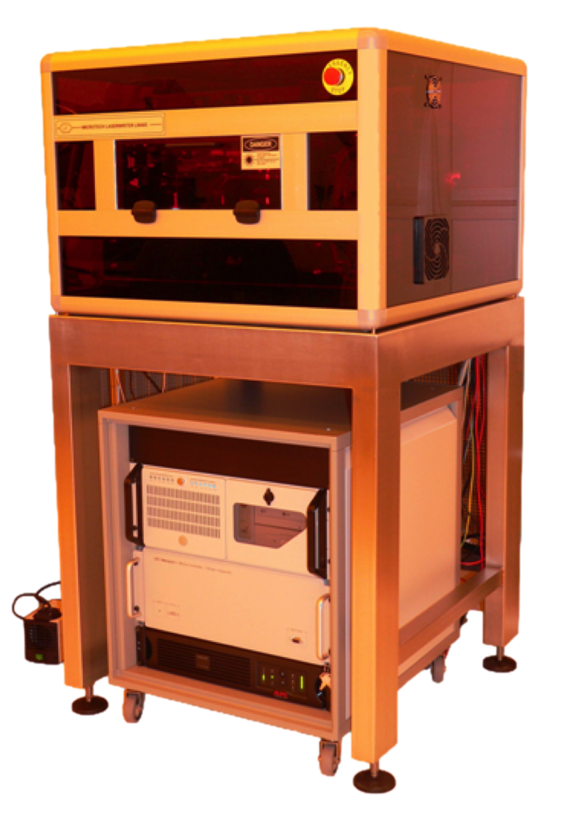
MICROTEC LW405B Laser Writer
MICROTEC LW405B Laser Writer
Easy to use, compact system for R&D labs and small volume production
-
-
-
-
Designed for definition of microstructures and surface diagnostics
System designed for resolutions down to 0.8µm
-
Writing tool for photolithographic mask fabrication of in-situ processing on planar substrates
System transform a laser beam into a controlled writing tool for mask fabrication of in-situ processing, eliminating the need for mask for lithography
-
-
-
Deep Reaction Ion Etching (DRIE)
Deep Reaction Ion Etching (DRIE)
Standard industry semiconductor etching purpose
-
-
-
-
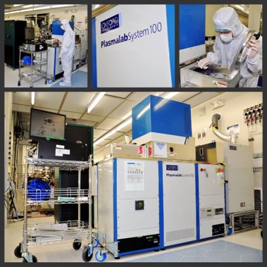
The Oxford Plasma Pro Cobra 100 Deep RIE uses special gases for standard industry semiconductor etching purpose. It is able to process both Bosch (chiller mode) and Cryo (liquid nitrogen mode) recipes for etching of silicon substrate. Apart from that, it can also etch oxides and nitrides. It has a load-lock and the process are completely computerized, robust and easy to use.
-
-
-
For an overview of our cleanroom equipment details, click here.
HOW IT WORKS?
Easy, 3 Step Process for Evaluation
STEP 01 |
STEP 02 |
STEP 03 |
||
 |
 |
 |
||
| Fill up inquiry form & Requirement discussion | Send us your sample | Test report delivered to your inbox |

