FRACTURE AND PLASTICITY AT THE NANOSCALES – IN SITU OBSERVATION DURING CLAMPED BEAM BENDING EXPERIMENTS of Cu/Nb NANOLAMINATES
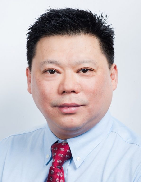
 Speaker: Dr. Arief Suriadi Budiman
 Affiliation: Extreme Materials Laboratory (XML), Singapore University of Technology & Design (SUTD)
Host: Professor Barbaros Oezyilmaz
Abstract Details: Plastic deformation mechanisms in metal-metal nanolayer composites (nanolaminates) have been studied extensively during the last decade, but their fracture responses (especially in an in situ set up) have not been reported. It has been widely observed that, for the case of metal-metal nanolaminates with a semicoherent interface, such as Cu/Nb, low interface shear strength increases the interface barrier to dislocation crossing, which improves nanolaminate plasticity. In this study, we use Cu(63nm)/Nb(63nm) accumulative roll-bonded nanolaminates, which have a large anisotropy of the interface shear strength between rolling and transverse directions (RD and TD, respectively), to study the effect of interface shear strength on the plasticity mechanisms and fracture events leading to the final catastrophic failure in metal-metal nanolaminates with a semicoherent interface during in situ clamped beam bending. Further, finite element analysis is used to understand the observed behavior. The results show a substantial difference between the fracture behaviors along the RD and TD owing to differences in the interface shear strength and grain size. For the RD beams, the slip bands originate from the Nb layers at the notch/crack tip followed by crack propagation along these bands. For the TD beams, the crack propagation is inhibited by interface shear. The results reveal that low interface shear strength can be utilized to improve fracture resistance in the studied nanolaminates, though weak grain boundaries can suppress the interface shear and the associated crack resistance improvement. This knowledge can be used to further optimize the nanolaminate fabrication process and achieve good strength, ductility, and crack resistance at the same time.
About The Speaker: Arief Suriadi Budiman received his B.S. in mechanical engineering from Institute of Technology, Bandung (ITB), Indonesia, his M.EngSc in materials engineering from Monash Univ., Australia and his Ph.D. in Materials Science and Engineering from Stanford University, CA in 2008. During his doctoral candidacy at Stanford’s Department of Materials Science & Engineering under the supervision of Professor William D. Nix (MRS Von Hippel Award 2007), Dr. Budiman received several research awards (MRS Graduate Silver Award 2006, MRS Best Paper 2006) and contributed to several high-impact journal publications (Acta Materialia, Applied Physics Letters, Journal of Electronic Materials). He gave two symposium invited talks as well in the MRS spring and fall meetings in 2006. More recently Dr. Budiman has been awarded the prestigious Los Alamos National Laboratory (LANL) Director's Research Fellowship to conduct top strategic research for the energy and national security missions of the Los Alamos National Laboratory's. At the Center for Integrated Nanotechnologies (CINT) at Los Alamos, Dr. Budiman’s research program involves nanomaterials for extreme environments with potential applications in advanced energy systems including for next-generation nuclear power reactors. Currently, at Singapore University of Technology & Design (SUTD), Prof. Budiman is leading a dynamic, young group researching nanomaterials and nanomechanics and their implications for extending the extreme limits of materials as well as their applications in the next generation energy technologies (solar PV, extreme environments, energy storage, etc.). His work has also recently received the famed Berkeley Lab Scientific Highlights twice in May 2010 and June 2013 (the latter was for his novel, innovative characterization technique that enables thin silicon solar PV technology). His deep expertise in the synchrotron X-ray microdiffraction technique was also recently utilized to enable the first ever in situ measurements of mechanical stresses in the 3-D through-silicon via (TSV) Cu interconnect schemes in the world – the findings were reported in a publication in Microelectronics Reliability (2012) and now one of the most highly cited references in the field of TSV/3D Interconnect stress measurements. He has been invited to give invited lectures/seminars on 3D/TSV Interconnect in various international conferences (including IEEE IITC 2012, AVS Thin Films Users Group 2012, TMS Symposium for Emerging Interconnects and Packaging Technologies 2011 and SEMATECH Workshop on 3D Interconnect Metrology at SEMICON 2011). Dr. Budiman has authored/coauthored several high-impact journal publications (Acta Materialia, Solar Energy Materials & Solar Cells, Materials Science Engineering A), and contributed a book chapter on “Electromigration in Thin Films and Electronic Devices: Materials and Reliability,” Woodhead Publishing, Cambridge, 2011. He has also recently published a book “Probing Crystal Plasticity at the Nanoscales – Synchrotron X-ray Microdiffraction” (Springer 2015). He has two U. S. Patents and one pending.
Click HERE for directions—
To view all the upcoming seminars, you can visit: https://graphene.nus.edu.sg/news-events/events/
You may also Like & Subscribe our following channels below to receive instant notifications for new announcements.
