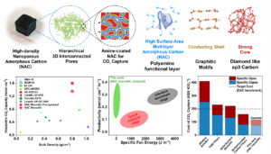
3D interconnected pore networks enable superior volumetric CO2 uptake in amine-functionalized nanoporous carbon for direct air capture
Our group has just published a paper on carbon capture!
What is perhaps most interesting about this work is that it did not begin with carbon capture at all. It started with a materials problem in supercapacitors in collaboration with Murata and eventually led us to a scalable all-carbon architecture that may now be relevant for direct air capture.
The material we developed is a high-density, all-carbon composite foam with a hierarchically interconnected porous network. Originally designed to support efficient charge transfer, it turns out that the same combination of conductivity, structural stability, and accessible surface area is also highly relevant for carbon capture systems.
Direct air capture faces a fundamental challenge: cost, driven in part by slow capture–release cycles and energy inefficiencies. Our approach explores Joule heating enabled by this material architecture, with the aim of accelerating these cycles and improving overall efficiency.
We are now developing this further through an LCER (Low Carbon Energy Research) Grant by A*STAR – Agency for Science, Technology and Research, including work toward a prototype system. It is still early, but preliminary data suggest that this route may reduce costs to below ~$200 per ton, with a possible path toward ~$100 per ton if the Joule heating concept can be validated at prototype scale.
For more information, see here.
“Breaking the 2-nm Barrier in Hard Disk Drives Using Monolayer Amorphous Carbon Overcoats” was made possible by a long-term collaboration with an industry partner, from early problem definition all the way through real manufacturing constraints. It is now accepted in Advanced Materials.
It also arrives at an inflection point for storage: AI is accelerating data growth in data centers, while the industry transitions to heat-assisted magnetic recording (HAMR). Together, these trends raise the bar for the media overcoat—demanding higher areal density and lower cost at scale, while tolerating repeated localized thermal cycling and still providing robust corrosion protection at ever-smaller thicknesses.
This project started more than 12 years ago, when Fuji Electric still had an HDD business and invited us to tackle what was then a fundamental—but not yet urgent—problem: the anti-oxidation barrier layer that ultimately limits areal density in hard disk drives (HDDs). We initially explored graphene, but both direct growth and transfer approaches ran into hard constraints set by thermal budget and surface roughness. Those dead ends forced us to rethink ultrathin carbon overcoats from the ground up, ultimately leading to the discovery of monolayer amorphous carbon (MAC) (Chee-Tat Toh et al., “Synthesis and properties of free-standing monolayer amorphous carbon,” Nature 577(7789), 199–203 (2020); https://lnkd.in/gsCQTzs6).
For data storage, this work is now advancing through close collaboration with a global technology leader in magnetic recording media, positioning the materials for real-world implementation.

For more information, see here.
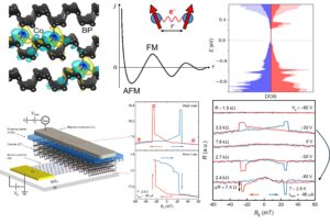
Our paper—“Electric field‑tunable ferromagnetism in a van der Waals semiconductor up to room temperature”—is now published in Nature Communications! This project took a long and winding path, and after more than five years and plenty of rethinking.
The 2D community is chasing perfection—cleaner crystals, sharper alignment, fewer defects. This work leans into the opposite idea: disorder.
In 2D, disorder can be surprisingly forgiving, e.g., carrier‑mediated (RKKY‑type) interactions are more long‑ranged and decay slowly, so doping can be minimized and doesn’t necessarily ruin the host. In black phosphorus, it allows cobalt to sit between the layers without destroying its semiconducting properties. Those moments interact, the gate tunes the interaction, and the result is induced ferromagnetism that is electrically tunable up to room temperature. Sometimes the trick isn’t making materials more perfect—it’s knowing how to use their imperfections.
For more information, see here.
Lithium-metal and anode-less batteries promise much higher energy density, but in reality they often struggle because lithium doesn’t deposit evenly on copper. That uneven plating leads to dendrites, dead Li, and early failure.
In our new paper in Advanced Science, we show that monolayer amorphous carbon (MAC)—a 2D material we pioneered—can change this behavior at the interface. A single-atom-thick, dopant-free layer turns copper uniformly lithiophilic, so lithium plates smoothly instead of forming whiskers or islands.
What excites us most is how simple and practical this is: an atomically thin coating, no doping, no thick interlayers, and direct compatibility with existing current collectors since MAC can be grown at ~ 200 °C. This makes it a promising route for anode-less lithium-metal batteries.
For more details, see here.
The transfer of large-area CVD graphene has long remained a limiting step in moving 2D materials from laboratory demonstrations to scalable device manufacturing.
In work now published in Advanced Materials, we demonstrate a fully dry, etchant-free, and automated transfer platform based on adhesion control using switchable ferroelectric polymers (PVDF-TrFE). By engineering interfacial forces through controlled polarization, graphene can be cleanly delaminated from copper and subsequently released onto target substrates without compromising material integrity. The process yields crack-free graphene with >99% coverage, avoids chemical etchants and polymer residues, and operates on minute-level cycle times. This method works equally for MoS2 and BN transfer.
![]()
More details at D. Zhang et al., Advanced Materials(2025)
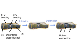
Silicon has long been considered one of the most promising anode materials for high-performance lithium-ion batteries due to its high theoretical capacity. However, a significant challenge that restricts its practical application is the persistent issue of weak interfacial contact in the silicon anode, which leads to structural instability during lithiation/delithiation processes due to large volume expansion. In this work, we develop a dual welding encapsulation strategy by constructing Si–C chemical bonding between the silicon and conductive covering shells and establishing C–C interlayer bonding connections among the covering shells. By directly examining the interface of silicon-based composites, we identify the types of compounds and hybrid orbital structures from their spatial distribution using machine-learning-enhanced transmission electron microscopy analysis techniques. This dual welding mechanism not only enhances the mechanical strength of the protective carbon shell but also ensures sustained electrical connection between the core and shell through the Si–C bonds. The robust heterogeneous structure effectively mitigates interfacial instability within the silicon anode, suppressing volume expansion below 12% after 300 cycles. Thus, the full-cell with the composite anode and LiNi0.8Co0.1Mn0.1O2 cathode performs a high energy density of 576 Wh kg–1 and stable cycling, inspiring the construction of commercial silicon batteries.
For more details, please refer to this link.
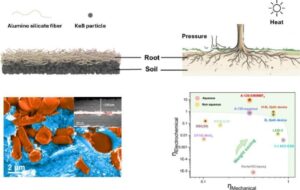
Structural supercapacitors, potential game-changers for various applications such as aerospace, automotive, and construction industries, offer a combination of energy storage and load-bearing functionalities. Conventional approaches, however, have been hindered by a significant decrease in overall energy storage performance due to the inherent separation of energy storage components and structural reinforcement elements. In this study, we report reinforcement-free all-in-one structural supercapacitors that tailor the conventional trade-off problem between energy capacity and mechanical strength by ensuring that the essential energy storage components possess high mechanical properties. This dual-functional structure ensures that it volumetrically constitutes nearly 90% of the cells excluding the packaging. Simultaneously, by employing interlocking interfacial engineering, we optimize the functionalities of these components, enhancing the overall robustness and energy capacity of the device. Consequently, our structural supercapacitor demonstrates good structural integrity, as evidenced by its flexural modulus of 8.34 GPa. Moreover, our supercapacitor stands out in terms of energy storage capacity, boasting a volumetric energy density of 45 Wh/L. This achievement, outperforming the current state-of-the-art by a staggering tenfold, significantly enhances multifunctionality, a critical index for evaluating structural energy devices, reaching a 9.95 rating. This novel strategy provides insight for other structural energy storage devices with higher multifunctional efficiency.
This is an international collaborative work. For more details, please refer to this link.
The incorporation of a SiC interfacial layer has been recognized as an effective strategy to tackle the interface contact issue between Si and carbon, ensuring the structural integrity of Si-based anodes and thereby enhancing their cycling stability. However, its inherent low activity and poor conductivity pose a persistent challenge for maximizing capacity and facilitating ion and electron transport. Here, we present a thickness/content adjustable SiC interfacial layer in the Si–SiC–C heterostructure using a modified spark plasma sintering technique. The SiC layer, with a content of ∼10%, is discretely coated on the surface of the Si core, exerting minimal influence on capacity and ion/electron kinetics, while ensuring high electrode structural stability. Consequently, the Si-based anode exhibits a stable capacity of 582 mAh g−1 (0.1 A g−1) and good rate capability (324 mAh g−1 at 2 A g−1), while maintaining 80% capacity retention over 500 cycles with a low electrode swelling of 12.6%. More importantly, its capacity presents a continuous rising trend with the increase of the cycle number, suggesting a mechanism where the SiC interfacial layer gradually transforms into a Li-ion-rich phase. This transformation facilitates ion transport and reaction with Si, resulting in gradual capacity enhancement. Therefore, the reasonably thickness-regulated SiC interfacial layer holds promise for providing inspiration for the design of commercial Si-based anodes.

This work is with several international collaborators. For more details, please refer to this link.
The single-atom thickness of graphene holds great potential for device scaling, but its effectiveness as a thin metal-ion diffusion barrier in microelectronics and a corrosion barrier for plasmonic devices is compromised by weak van der Waals interactions with copper (Cu), leading to delamination issues. In contrast, monolayer amorphous carbon (MAC), a recently reported single-atom-thick carbon film with a disordered sp2 hybridized structure, demonstrates superior adhesion properties. This study reveals that MAC exhibits an adhesion energy of 85 J m−2 on Cu, which is 13 times greater than that of graphene. This exceptional adhesion is attributed to the formation of covalent-like Cu─C bonds while preserving its sp 2 structure, as evidenced by X-ray photoelectron spectroscopy (XPS) and near-edge X-ray absorption fine structure(NEXAFS) spectroscopy. Density functional theory (DFT) calculations further elucidate that the corrugated structure of MAC facilitates the hybridization of C 2p z orbitals with Cu 4s and 3dz 2 orbitals, promoting strong bonding. Theseinsights indicate that the amorphous structure of MAC significantly enhances adhesion while preserving its elemental composition, providing a pathway to improve the mechanical reliability and performance of two-dimensional(2D) materials on metal substrates in various technological applications.

This work is with several international collaborators. For more details, please refer to the link.
Despite the superior properties of two-dimensional (2D) materials, their low fracture toughness has limited practical applications. Our study demonstrates intrinsic toughening in monolayer amorphous carbon (MAC) nanocomposites predominantly composed of amorphous phases with small crystalline domains, showing significant enhancements in energy absorption during crack propagation. These improvements are quantitatively investigated through in situ SEM tensile testing and molecular dynamics (MD) simulations. This work not only unveils the toughening mechanisms but also introduces an intrinsic toughening strategy for 2D materials, enabling their use in fields requiring robust fracture resistance.
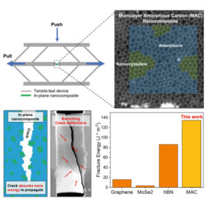
This work is with several international collaborators. For more details, please refer to the link.