Upconversion electroluminescence in 2D semiconductors integrated with plasmonic tunnel junctions
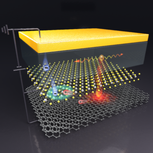
Plasmonic tunnel junctions are a unique electroluminescent system in which light emission occurs via an interplay between tunnelling electrons and plasmonic fields instead of electron–hole recombination as in conventional light-emitting diodes. It was previously shown that placing luminescent molecules in the tunneling pathway of nanoscopic tunnel junctions results in peculiar upconversion electroluminescence where the energy of emitted photons exceeds that of excitation electrons. Here we report the observation of upconversion electroluminescence in macroscopic van der Waals plasmonic tunnel junctions comprising gold and few-layer graphene electrodes separated by a ~2-nm-thick hexagonal boron nitride tunnel barrier and a monolayer semiconductor. We find that the semiconductor ground exciton emission is triggered at excitation electron energies lower than the semiconductor optical gap. Interestingly, this upconversion is reached in devices operating at a low conductance (<10−6 S) and low power density regime (<102 W cm−2), defying explanation through existing proposed mechanisms. By examining the scaling relationship between plasmonic and excitonic emission intensities, we elucidate the role of inelastic electron tunnelling dipoles that induce optically forbidden transitions in the few-layer graphene electrode and ultrafast hot carrier transfer across the van der Waals interface.

This work is lead by Prof. Goki Eda’s group with contribution from Prof. Barbaros’ group. For more details, please refer to the link.

