
Since 2008 we have been working towards exploring the potential uses of graphene in a wide range of areas. This effort accelerated in 2010 with our demonstration of the first graphene based touch panels [Nature Nano.]. After receiving a prestigious S$ 10 million CRP grant (“Towards Commercialization of Graphene Technologies” , WBS No. – R-144-000-315-281) our group became even more concentrated in translating our discoveries in basic science into patents and building industry relevant know how. Below is a summary of our areas of interest.
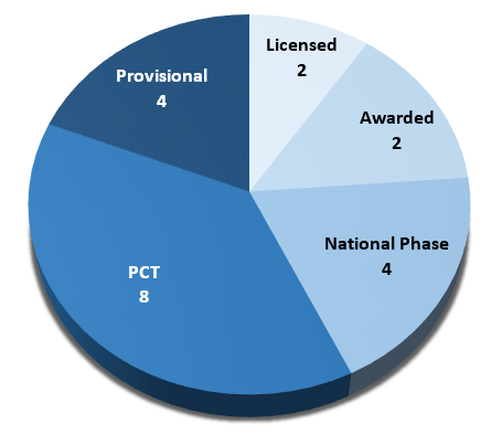
PATENT DISTRIBUTION BY STATUS
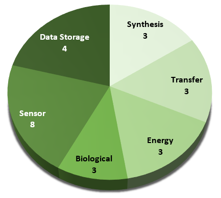
PATENT DISTRIBUTION BY FIELD
AWARDED AND/OR LICENSED
Gate-tunable graphene-ferroelectric hybrid structure for photonics and plasmonics
Abstract: The invention relates to a novel type of gate-tunable photonics and plasmonics which utilizes doped large-scale graphene coupled with ferroelectric material. The graphene-ferroelectric hybrid structure paves the way for the realization of ultra-fast, low power consumption and multi-wavelength operation saturable absorbers for applications in ultra-fast laser systems and novel types of plasmonics for applications in infrared detection, single-photon quantum devices and ultrasensitive detectors.
Patent number: US9184553
Filed: June 6, 2013
Date of Patent: November 10, 2015
Assignee: National University of Singapore
Inventors: Barbaros Özyilmaz, Guang Xin Ni, Yi Zheng
Also published as: EP2859628A1, EP2859628A4, US20150155681, WO2013184072A1
Abstract: A transparent conductor comprising: a graphene layer and a permanent dipole layer on the graphene layer configured to electrostatically dope the graphene layer.
Patent number: US9082523
Filed: November 10, 2011
Date of Patent: July 14, 2015
Assignee: National University of Singapore
Inventors: Barbaros Özyilmaz, Guang Xin Ni, Yi Zheng
Also published as: CN103201106A, CN103201106B, EP2637862A1, EP2637862A4, US9082523, WO2012064285A1
Electronic devices based on current induced magnetization dynamics in single magnetic layers
Abstract: The present invention generally relates to magnetic devices used in memory and information processing applications, such as giant magneto-resistance (GMR) devices and tunneling magneto-resistance devices. More specifically, the present invention is directed to a single ferromagnetic layer device in which an electrical current is used to control and change magnetic configurations as well as induce high frequency magnetization dynamics. The magnetic layer includes full spin-polarized magnetic material, which may also have non-uniform magnetization. The non-uniform magnetization is achieved by varying the shape or roughness of the magnetic material. The present invention may be used in memory cells, as well as high frequency electronics, such as compact microwave sources, detectors, mixers and phase shifters.
Patent number: US7986544
Filed: November 5, 2007
Date of Patent: July 26, 2011
Assignee: New York University
Inventors: Andrew Kent, Barbaros Özyilmaz
Also published as: CA2668351A1, EP2089888A2, EP2089888A4, EP2089888B1, US20110038198, WO2008115291A2, WO2008115291A3
Locally gated graphene nanostructures and methods of making and using
Abstract: A locally gated graphene nanostructure is described, along with methods of making and using the same. A graphene layer can include first and second terminal regions separated by a substantially single layer gated graphene nanoconstriction. A local first gate region can be separated from the graphene nanoconstriction by a first gate dielectric. The local first gate region can be capacitively coupled to gate electrical conduction in the graphene nanoconstriction. A second gate region can be separated from the graphene nanoconstriction by a second gate dielectric. The second gate region can be capacitively coupled to provide a bias to a first location in the graphene nanoconstriction and to a second location outside of the graphene nanoconstriction. Methods of making and using locally gated graphene nanostructures are also described.
Patent number: US8659009
Filed: October 31, 2008
Date of Patent: February 25, 2014
Assignee: The Trustees of Columbia University in the City of New York
Inventors: Barbaros Özyilmaz, Dmitri Efetov, Pablo Jarillo-Herrero, Philip Kim
Also published as: US20090140801
High speed low power magnetic devices based on current induced spin-momentum transfer
Abstract: The present invention generally relates to the field of magnetic devices for memory cells that can serve as non-volatile memory. More specifically, the present invention describes a high speed and low power method by which a spin polarized electrical current can be used to control and switch the magnetization direction of a magnetic region in such a device. The magnetic device comprises a pinned magnetic layer with a fixed magnetization direction, a free magnetic layer with a free magnetization direction, and a read-out magnetic layer with a fixed magnetization direction. The pinned magnetic layer and the free magnetic layer are separated by a non-magnetic layer, and the free magnetic layer and the read-out magnetic layer are separated by another non-magnetic layer. The magnetization directions of the pinned and free layers generally do not point along the same axis. The non-magnetic layers minimize the magnetic interaction between the magnetic layers.
Patent number: US6980469
Filed: August 19, 2003
Date of Patent: December 27, 2005
Assignee: New York University
Inventors: Andrew Kent, Enrique Gonzalez Garcia, Barbaros Özyilmaz
Also published as: CA2535965A1, EP1665388A2, EP1665388A4, EP2503613A2, EP2503613A3, EP2503614A2, EP2503614A3, US7170778, US7307876, US20050041462, US20060030058, US20070030728, WO2005020251A2, WO2005020251A3